Research
The scientific roots of DEIB research activities in Electronics date back to 1957 when Emilio Gatti was appointed to the first Professorship of Electronics in Italy. Following his vision, Electronics research at DEIB has always been carried out through a balanced mix of theoretical analysis and experimental activities.
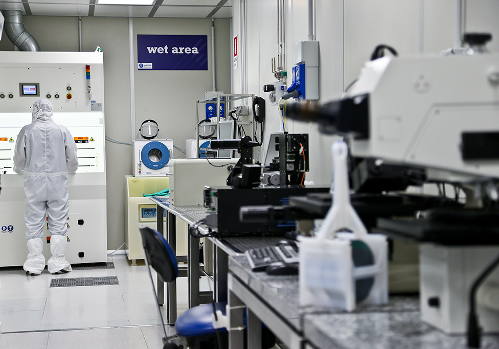
Today, the research activity is carried out in 1400 square meters of laboratories equipped with state-of-the-art tools to design, simulate, and characterize the electrical and optical properties of a broad range of nano- and opto-electronic devices, sensors, integrated circuits, and systems. Devices and integrated circuits are fabricated either in the University’s clean room, PoliFab, or in collaboration with major semiconductor companies and research institutions.
A Faculty of 23 professors, supported by more than 60 Ph.D. students and post-doc researchers, teaches about forty courses on various subjects of Electronics Engineering at undergraduate and graduate level.
The research activities are organized in the following major lines
- Electron Devices
- Smart Microsensors and Microsystems
- Electronic Circuits Design
- Single-Photon Detectors
- Radiation Detectors
- Digital Systems
Electron Devices
The research line addresses current and emerging electron devices and technologies, with activities in two main fields:
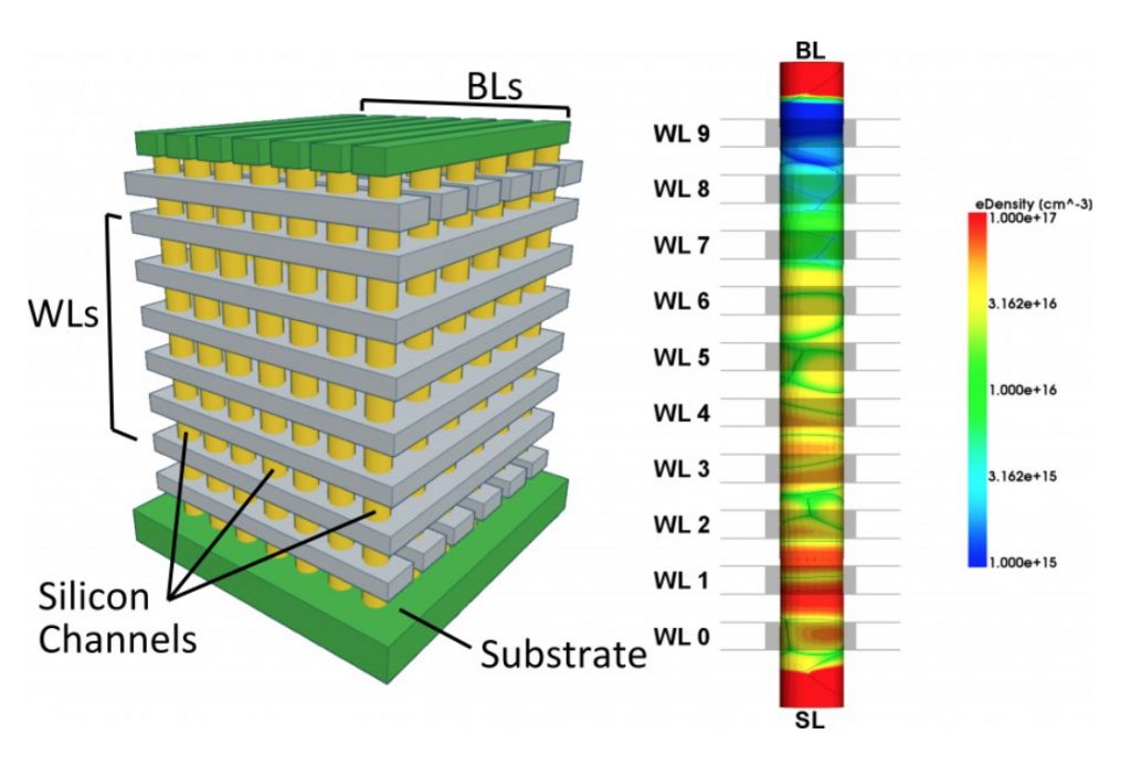
Nano-electronic devices and technologies for high-density data storage and in-memory computing: Solid-state memories have been playing an increasingly important role in the world of electronics, thanks not only to the large variety of applications currently arising from the unprecedented bit storage density of nanoscale technologies but also to the prospects of new memory-enabled computing paradigms on the horizon. In this context, the research activities are mainly focused on the experimental and numerical investigation of the basic physics, the reliability and the performance of nano-electronic devices for high-density data storage and in-memory computing. 3D-NAND Flash, NOR Flash, Phase-Change Memories (PCM), Resistive Random Access Memories (ReRAM), Magnetoresistive Random Access Memories (MRAM) and Ferroelectric Memories are just the most relevant investigated technologies. Among the major aims of the research, it is worth mentioning the understanding of the basic phenomenology, the main dependences and the impact on the technology of the variety of physical phenomena taking place in solid-state nano-electronic devices for high-density data storage, exploring also the possibility to exploit these devices for the emerging in-memory computing scenarios. The work is carried out in collaboration with some of the most important semiconductor companies in the world, among which it is worth mentioning Micron Technology Inc. and STMicroelectronics, or under the framework of national and international research projects.
Organic semiconductor devices: organic semiconductor devices, aiming to develop optotelectronic devices and systems on plastic substrates by means of solution-based, low thermal budget, highly scalable techniques (such as inkjet printing, spray-coating etc.).
Most relevant recent achievements are:
- Nano-electronic devices and technologies for high-density data storage and in-memory computing
Activities performed in this field are constantly pushing forward the frontiers of knowledge on nano-electronic devices and technologies, contributing to the successful trends of solid-state memories for high-density data storage and promoting the development of new memory-enabled computing paradigms. The results achieved by the research line have shed light upon many aspects related to the reliability, performance and prospects of the most relevant state-of-the-art and emerging solid-state memory devices and technologies. Among them, it is worth mentioning the internationally recognized achievements on the experimental characterization and the theoretical modeling of program noise, charge detrapping and random telegraph noise in Flash memories and of resistive switching, data retention and endurance in ReRAM and PCM. Besides, leading-edge results have also been reported on the possibility to exploit nonvolatile memory arrays either as synaptic arrays in supervised and unsupervised artificial neural networks or as computing elements in new, fast and low-power electronics systems. - Devices based on organic semiconductors The research has contributed to the analysis of carrier transport and of light-matter interaction phenomena in organic semiconductors. In the field of polymeric transistors, the correlation between carrier mobility, energetic disorder and molecular weight has been addressed. The issue of contact resistances in organic transistors has been modelled and analyzed. From the technological point of view, the encapsulation of organic transistors by means of Atomic Layer Deposited Aluminum Oxide has been demonstrated. In the field of organic photodetectors, a multilayer device architecture to suppress dark currents via injection blocking layers has been devised. Photodetectors sensitive to the Vis-NIR have been demonstrated. The indirect detection of X-rays, aimed at biomed applications, has been explored. Efforts are now directed toward the realization of pixels and matrices thereof by means of scalable, printing techniques (such as inkjet printing), aimed at developing large area image sensors on plastic substrates. In addition, in the framework of a collaboration with the Dipartimento di Matematica of Politecnico di Milano, the simulation and parameter estimation of organic-based devices is now under development.
Smart Microsensors and Systems
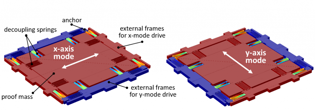
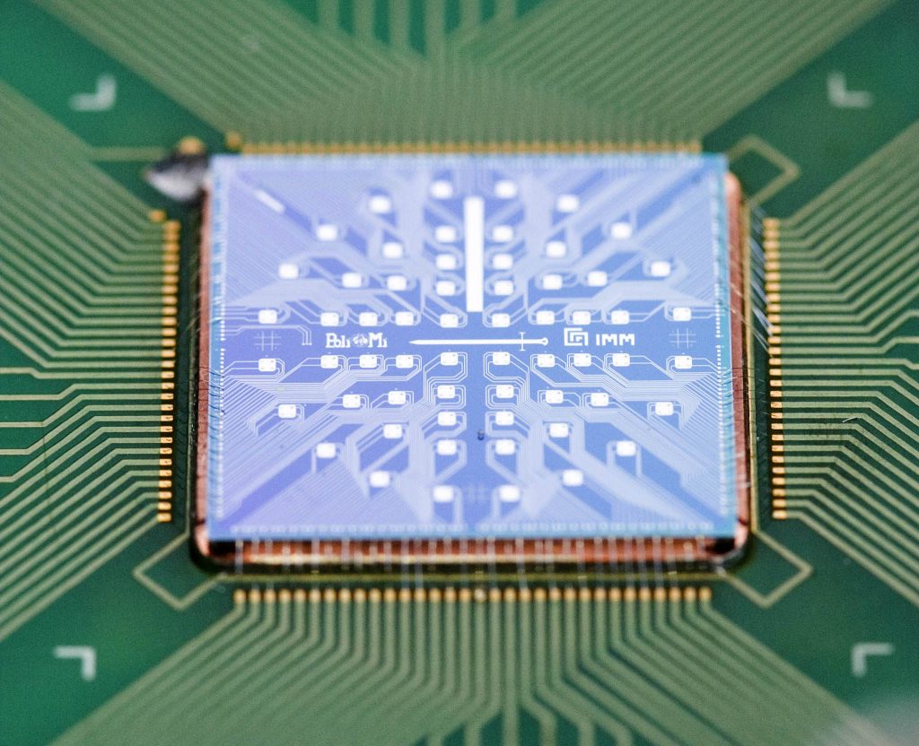
The research activity carried out at the Politecnico di Milano on microsensors and intelligent microsystems covers a wide range of aspects ranging from the study of the physical principles of operation of these devices to the study of the properties of the materials of which they are made, from the design of the device itself to that of the electronics to which it is connected, from laboratory testing to the development of related applications. Two main types of devices are currently the focus of interest of the research group: the first concerns inertial multi-axis sensors and multi-parameters M/NEMS (Micro/Nano Electro-Mechanical Systems), the other concerns CMOS image sensors with tunable spectral response in the visible spectrum and near infrared.
Among the main results we remember:
- Development of innovative MEMS accelerometers and reading and signal conditioning electronics
In the framework of two CARIPLO projects and consolidated industrial collaborations with STMicroelectronics, fundamental properties of micro-scale materials used in MEMS have been studied, such as fatigue effects, surface adhesion phenomena and nonlinear effects. The results have been used for the design of innovative resonant MEMS sensors, typically subject to a very large number of cyclic stresses during their lifetime. - Development of CMOS image sensors with electrically tunable spectral response
A new CMOS image sensor with electrically-configurable spectral response at single pixel level was invented, designed and subsequently tested by the researchers of the group. During the research, problems at the device level have been analyzed and solved, the operation of the sensor has been experimentally demonstrated and new features have been proposed, such as the adaptation of the sensor to the scene, the acquisition of multi-spectral images and the possibility of simultaneous acquisition of the image in the visible and near infrared. - Development of advanced gyros based on nano-structured functional elements integrated in micro-structured devices (N/MEMS)
As part of an international EU project (NIRVANA), the research group had the task of designing advanced miniature gyroscopes in which the reading of the Coriolis Force is based on the piezo-resistive properties of nano-structured functional elements. The first prototypes of these sensors were produced (at CEA-LETI in Grenoble) and were characterized by the research group with very satisfactory results. - Development of drive and reading electronics for MEMS/NEMS
The MEMS/NEMS sensor design is closely linked to the design of the relevant drive and read electronics. The research group covers both activities. Several integrated circuits for MEMS and measuring instruments for their characterization have been developed. In particular, a versatile platform for the complete characterization of MEMS/NEMS has proved to be of relevant industrial interest.
Electronics circuits design
This research line is focused on the design of fully-integrated circuits in Silicon (Application Specific Integrated Circuits, ASIC). The modern technological process in CMOS technology make available transistors on a nanometric scale (e.g. minimum size of few nanometers), that allows to process digital signal at unprecedented speed, cramming at the same time millions of transistors in few mm square. On the other hand, the performance of the unavoidable analog circuits, such as accuracy and noise, are degraded.
Full integration in silicon of high performance systems, such as the ones for future wireless standard (5G), low power sensors (IoT), mmw radar for autonomous cars and smart sensors, calls for a new design paradigm, in which the digital processing is exploited to compensate the analog impairments, and, in general, to improve the overall performance. Within themes collaborations are active with research centers in universities and semiconductor companies, such as Infineon Technologies, STMicroelectronics, Intel.
- Probably the main research theme is the design of integrated circuits for frequency synthesis, based both on Phase-Locked Loops (PLLs) and Multypling Delay-Locked Loop (MDLLs), mainly in CMOS technologies. The research group has proposed several design innovations, substantially improving the state of the art, architectural and it is recognized as one of the leading groups at international level. As an example in the RF area, PLLs operating between 1 and 30 GHz have been designed for wireless applications, such as WiFi, LTE, 5G, IoT, in which background digital calibrations (embedding more than 20 thousands of gates) allows reaching unprecedent jitter-power performance, i.e. a time error around 100-300 fs, with a low power budget (4 – 10 mW). These techniques have been applied recently to the implementation of both 77 GHz FMCW radar and point-to-point communications in E-band (80GHz) and to Iot network sensors.
- A new research area is the design of digitally-intensive RF Power Amplifier (PA). New techniques are studied to improve the PA efficiency, the amin application being the sensors networks for IoT, where battery life is a bottleneck.
- Related to the frequency synthesis is the research on fundamental of phase noise in oscillators, and in injection-locked circuits, both for frequency division and multiplications. The group has been active in this area for two decades and has proposed several design solution to improve the state of the art in term of phase noise.
- Another area in which important results have been achieved is the design of fully integrated CMOS systems for sensorsapplications. These systems have been employed in the neural recording, for medical applications, and as a front-end in MEMS (Micro Electro-Mechanical Sensors) systems, embedded in magnetometers, accelerometers, gyroscopes etc… The main challenge in these design is the low-power low-noise signal detection and its analog-to-digital conversion.
Single-photon detectors and applications
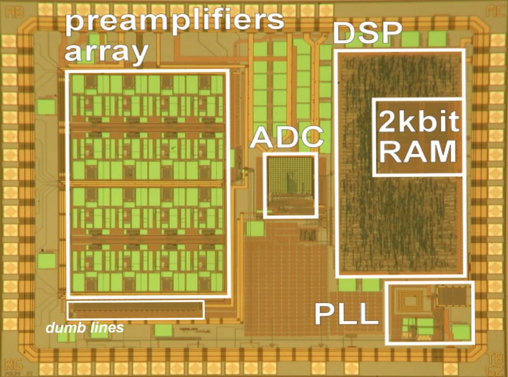
The activity is focused on the development of single-photon avalanche diodes (SPADs) and associated electronic instrumentation and systems for low-light-level detection, with special attention to applications in life-science, such as micro- and nano-analytical techniques for biomedical and genetic diagnostics, and high-sensitivity and high frame-rate imaging, like 2D spectroscopy and 3D time-of-flight ranging. A driving force is the widespread interest to rapid and efficient detection of fluorescent emission from extremely small biological samples down to single molecules of DNA and proteins. Main goal is the development of new miniaturized detection systems that overcome drawbacks and limitations of existing systems, which rely on bulky and costly equipment and discrete sensors. High attention and remarkable efforts are devoted to imaging with ultrafast time-resolved capability at single-photon level with array detectors in linear and 2D geometries.
- Resonant-cavity-enhanced (RCE) SPAD detectors
We developed the first RCE SPAD detectors on a reflecting silicon-on-insulator (SOI) substrate. The substrate incorporates a two-period distributed Bragg reflector, developed in collaboration with Boston University. The RCE SPAD detectors have peak photon detection efficiency (PDE) ranging from 42% at 780 nm to 34% at 850 nm and time resolution of 35 ps full-width at half-maximum. These detectors are suitable for demanding photon-counting applications, where both high PDE and picosecond time resolution are required. - Fully-programmable 1.55µm photon-counting module for InGaAs/InP SPADs
We conceived, designed, fully characterized and validated in actual experiments a state-of-the-art near-infrared photon-counting module. The module exploits at best the performance of InGaAs/InP SPADs for detection of very fast and faint optical signals in the near-infrared range up to 1.7 μm; it is flexible and suitable for various advanced applications thanks to a user-friendly interface and a user-adjustable setting of all parameters. We validated the actual electronics and detector performance in nanosecond-gated operation up to 133 MHz gate repetition frequency, verifying excellent photon-timing performance (time jitter better than 100 ps) and detector operation at controlled low temperature. - CMOS SPAD imagers for 2D single photon counting
We developed cost-effective fully-CMOS compatible SPAD arrays in a 0.35µm CMOS technology. The array has smart-pixels composed by a SPAD detector, analog sensing and avalanche quenching electronics, in-pixel digital processing for counting the incoming photons and in-pixel memory and buffer stages for global-shutter readout with no dead-time. A 64×32 SPAD imager can acquire 2D images and 2D videos up to 100,000 frames/s with 8bit photon-counting dynamics. A 32×1 array provides 50ps resolution in photon-timing. The advanced performances have already enabled new scientific results, like sub-Reyleigh imaging via N-photon detection and advanced in Fluorescence Lifetime Imaging (FLIM) and Diffuse Optical Tomography (DOT) applications.
Radiation detectors and applications
The group carries out research for the development and application of semiconductor detectors for ionizing radiation and particles, together with their dedicated electronics. The focus is both on the study and design of new types of detectors and on the configuration, characterization, and application of detectors in different fields of science and technology. The group follows the entire development path from the detector, to the required front-end and back-end electronics, to the prototyping of systems to be used in research projects or in user-oriented applications. The group is active in interdisciplinary experiments in Nuclear Physics, Materials Science, Biomedical Engineering and Nanotechnologies.
Main results of the research
- Development of high-resolution gamma-ray imaging devices for nuclear medicine
High resolution gamma-ray detectors have been developed for applications in nuclear medicine, gamma astronomy and nuclear physics. The detectors are based on the readout of scintillators with Silicon Drift Detector (SDD). Advantages: better resolution than traditional photomultiplier tubes, insensitivity to magnetic fields, compactness, low polarization voltage. In the framework of the EU HICAM project, an SDD-based gamma chamber has been developed and validated in clinical studies. - Design and characterization of an innovative instrument for X images in fluorescence and diffraction, based on polycapillary optics and on an energy-sensitive image sensor
An innovative X-ray fluorescence and diffraction imaging tool has been developed and successfully applied. Its special features are the use of polycapillary optics instead of mechanical collimators for angular selection, which allows for increased efficiency, the illumination of the sample with an X-ray tube and the detection of emitted and diffused radiation through an energy-sensitive image sensor that avoids the use of synchrotron light. - Achieving maximum electron drift velocity in multilinear silicon drift detectors (MLSDDs) and their application in astronomical applications
We have designed and fully characterized prototypes of MLSDD detectors capable of operating at very high drift speeds. This is the highest drift rate ever measured in silicon drift detectors. A prototype of a Compton imaging scatter detector has been successfully developed for space applications, capable of tracking electrons in a single layer of detection. - The first high-resolution X-ray detectors based on silicon carbide (SiC) were developed as part of a collaboration involving the Universities of Bologna, Firenze, Modena, Torino and the Selex Integrated System company. Schottky and ohmic junction technologies have been developed in order to obtain dark current densities more than two orders of magnitude smaller than in any other semi-conductor detector. This allowed to implement SiC pixel detectors with the capability of sub-electronic noise at room temperature without the need of cooling systems, and the acquisition of high-resolution X spectra with the detectors at a temperature of +100°C.
- -Development of digital instrumentation for adaptive filtering in demanding measurements
Taking advantage of the increasing performance of modern analog-to-digital converters and the processing speed of FPGAs and DSPs, digital systems for spectroscopy have reached high potentialities making use of linear and non-linear minimum square-weighted algorithms for very high resolution energy measurements and eventual occurrence time, and adaptive filtering at the single pulse level. The power of digital processing has allowed the development of innovative tools for physical and biomedical research.
Digital systems
The research is focused on the study and development of digital signal processing architectures in VHDL and Verilog environments. This approach leads to the description of circuit structures that can be implemented both in configurable electronic devices (DSP, FPGA, SoC-Linux based) and in ASIC circuits. The first implementation choice is indicated for prototyping digital circuits and systems and when the reconfigurability property is a key factor in the application to which the processing architecture is intended. The second solution of implementation is pursued when performance targets are required or when the application corresponds to large production volumes.
In this perspective, the research activity mainly concerns the development, prototyping and engineering of digital architectures in hardware, firmware and software aspects for high-performance digital processing of signals and data with massive algorithmic treatments in real time.
Most of these activities are set in research contracts and collaboration agreements with national and international scientific institutions and have produced over three hundred publications in journals and international conference proceedings.
Mainstreams of the research are:
- “Time-Mode” Circuits and Systems
“Time-mode” circuits represent the information by time difference between digital events. In these circuits the time-to-digital converter (TDC) is a basic component, i.e. a system for mapping a time variable to a digital code. Present and above all future applications of these circuits are vast and transversal to many scientific and industrial sectors, from LIDAR systems in automotive and cybernetics (Smart Mobility, Industry 4.0) to medical imaging systems as SPECT and PET (Health), from time-of-flight cameras for industry (Industry 4.0) to laser scanning systems for industry automation (Industry 4.0), just to name a few. Key enabling technologies for these circuits are field-programmable gate array (FPGA) devices. It is well-known that the implementation can be performed both in digital ASICs and in FPGAs. Of course, the realization in FPGA is by far preferable due to extremely lower development costs and higher flexibility of the implemented architectures thanks to the programmable resources of the device. This is even more true because the huge evolution of FPGA devices is reducing more and more the gap of performance with respect to ASIC counterparts. The research deals particularly with the development of innovative high-performance TDC architectures designed for FPGA and SoC devices, several of which are acknowledged as solutions beyond the state-of-art. - Power Electronics
Mainstreams have been digital control of DC-DC converters for low power supplies, development of innovative solutions for digital control of charge-discharge processes in the storage cells used in high-stress operating conditions, such as in vehicular electric traction. New architecture combining the high-power density of supercapacitors with the high energy density of lithium-ion cells have been developed and tested. Also, investigation on digital energy management systems in the “distributed generation” has been carried out, in which devices within the distribution system can be both users and generators. The results are also applied in the field of renewable energy sources, in particular photovoltaics. - Radiation detectors: methods for optimum digital signal processing
The group has been studying methods for digital processing of signals from radiation detectors since 1992. Specifically, the milestones are the study and experimental realization of DSP methodologies for the real-time multi-channel processing of data from radiation detectors; the study and realization of optimal digital filters adapted to the waveforms of the signals and to the actual noise associated with the signal; algorithms for estimating waveforms and methods for determining weight functions in the presence of time and frequency constraints; waveform analysis methods; DSP techniques designed for operating in real time and simultaneously adaptive to changes in the characteristics of the experimental setup.