Alumni
Here are some of our former graduated students, who reached outstanding positions in different fields and environments, both in Italy and abroad. As you can see, Electronics engineers boost excellence everywhere!
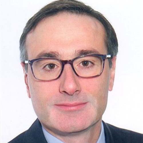
Alberto Sangiovanni-Vincentelli. I was born in Milano in 1947. I received an MS in Electronic Engineering cum laude from Politecnico di Milano in 1971. After graduation, I joined the Department of Electronic Engineering as a researcher first and then as a Professore Incaricato. In 1975, I joined Electrical Engineering and Computer Sciences at the University of California, Berkeley, where I hold the Edgar L. and Harold H. Buttner Chair. Among various visiting positions, I was at IBM T.J. Watson Research Center in 1980 and at MIT in 1987. In 2001, I received the Kaufman Award for my pioneering contributions to EDA from the Electronic Design Automation Consortium. In 2011, I was awarded the IEEE/RSE Maxwell Medal “for groundbreaking contributions that have had an exceptional impact on the development of electronics and electrical engineering or related fields”. I co-founded Cadence and Synopsys, listed in NASDAQ with market cap of over 40 Billion USD. I presently serve on the Board of Directors of Cadence Design Systems, KPIT (India), Cogisen, ISEO, Expert System (Italy), and UltraSoC (UK) (Chairman of the Board). I consulted for, among others, Intel, HP, TI, ST Microelectronics, Mercedes, BMW, Magneti Marelli, Telecom Italia, United Technologies, Camozzi Group, Pirelli, General Motors, UniCredit and UnipolSAI. I had been the President of Comitato Nazionale dei Garanti per la Ricerca and President of the Strategy Committee of the Fondo Strategico Italiano. I am also serving as member of the Advisory Board of the Politecnico di Milano, and as Chairman of the International Advisory Council of MIND (Milano Innovation District). I am a member of the United States National Academy of Engineering, an IEEE and ACM Fellow. I received an honorary Doctorate from Aalborg University (Denmark) and one from KTH (Sweden). I published more than 950 papers and 19 books.
Mario Caironi was born in Bergamo (Italy) in 1978. He studied at “Politecnico di Milano” (Milan, Italy) where he obtained his Laurea degree in Electrical Engineering in 2003 and a Ph.D. in Information Technology with honours in 2007, with a thesis on organic photodetectors and memory devices. In March 2007 I joined the group of Prof. Henning Sirringhaus at the Cavendish Laboratory (Cambridge, UK) as a post-doctoral research associate. I worked in Cambridge for 3 years on high resolution inkjet printing of downscaled organic transistors and logic gates, and on charge injection and transport in high mobility polymers. In April 2010 I was appointed as a Team Leader at the Center for Nano Science and Technology@PoliMi of the Istituto Italiano di Tecnologia (Milan, Italy). In 2014 I entered the tenure track at the same institution, securing a tenured Senior Researcher position in 2019. I am currently responsible of the “Printed and Molecular Electronics” research line and my group is currently composed of 7 postdocs, 8 PhD students and 1 fellow researcher. I am author and co-author of more than 120 scientific papers in international journals and books. I have an h-index of 35 (Scholar – July 2019). I am currently interested in solution based high resolution printing techniques for micro-electronic, opto-electronic and thermoelectric devices fabrication, in the device physics of organic semiconductors based field-effect transistors and their integration in high-frequency printed circuits, and in biomedical and/or implantable sensors and electronics for the healthcare. I am an 2014 ERC grantee.
My double-E master degree at POLIMI was key to the rest of my career. When I joined the Cavendish Labs, I immediately teamed with chemists and physicists who were developing the fastest polymer transistor at that time. They did not know how to measure it. I went back to my university notes, and found very soon the solution. A few months later we published a paper that is still, after 10 years, a milestone in polymer electronics. I believe that as research fields become more and more inter- and multi-disciplinary, with impact on healthcare and personalized medicine, it is even more important to hold solid basis in one sector to be able to make a difference: and Electronics is everywhere! As such, a double-E degree will give you the keys to many future technologies.
Franco Stellari (S’95–M’04-SM’06) received the M.S. degree (summa cum laude) and the Ph.D. degree in electronics engineering from the Politecnico di Milano, Milan, Italy, in 1998 and 2002 respectively. He subsequently joined the IBM T.J. Watson Research Center in Yorktown Heights, NY as a post-doc, becoming a permanent Research Staff Member in 2004. His major interest is the development and use of new optical techniques for testing VLSI circuits based on static imaging, time resolved emission and laser based techniques. During the years he has worked with single-photon detectors with fast response time and very high quantum efficiency, such as InGaAs Single Photon Avalanche Diodes (SPADs) and Superconducting Single Photon Detectors (SSPD), pushing their limits towards record low voltage applications. In 1999 he developed a model of the emission that is still currently used for estimating luminescence from electric circuits. He has also developed a novel methodology for studying latch-up ignition, process variability, and electric signal characteristics. More recently, he has worked on fully exploiting the Light Emission from Off-State Leakage Current (LEOSLC) to developed novel techniques for VLSI circuit testing and hardware security such as process variability measurement, power supply noise measurement, chip alterations detection, and logic state mapping, chip reverse enginnering, etc. He has about 100 international publications, more than 30 granted patents, and several more pending. He won the Paul F. Forman Team Engineering Excellence Award in 2015, IEEE EDS Paul Rappaport Award for the best Trans. on Electron Devices of 2004, Best Poster Award at the International Symposium for Test and Failure Analysis (ISTFA) in 2014, and the Best Paper Awards at the European Symposium on Reliability of Electron Devices, Failure Physics and Analysis (ESREF) twice, in 2002 and 2004.
Irene Perali Born and raised in a small town new Brescia, in 2006 I moved to Milan to study engineering at Politecnico di Milano. I completed a Bachelor degree in Biomedical Engineering and a Master degree in Electronics Engineering in 2009 and 2011, respectively. After that, I enrolled in a Ph.D. program in the Radiation Detector Laboratory and graduated in 2015 with a thesis on the development of a gamma camera for Proton Therapy applications. In 2015, I joined Apple Special Project Group to work as a Systems Engineer on new sensing technologies for autonomous systems. After a short period spent at the Apple offices in Zurich, late in 2015 I moved to the headquarters in Cupertino, California.In 2019 I left Apple to join Zoox, a start-up founded in 2014 and based in Foster City. The company mission is to create fully autonomous mobility from the ground up. I currently lead Systems Engineering and Functional Safety activities for the sensors organization, working on different sensing modalities like Cameras, Lidars and Radars.My coursework at Politecnico didn’t include subjects related to autonomous vehicles, but during my master in electronics I learned a method to approach complex systems with an intuitive approach, a skill particularly useful in the super-fast working environment of Silicon Valley.
My coursework at Politecnico didn’t include subjects related to autonomous vehicles, but during my master in electronics I learned a method to approach complex systems with an intuitive approach, a skill particularly useful in the super-fast working environment of Silicon Valley.
My Ph.D research gave me the opportunity to go through an end-to-end process of prototype development, from requirements to design, build and testing. This gave me a mindset that will always support me in my career path.
Agostino Pirovano was born in Italy in 1973. I received the M.S. in Electronic Engineering cum laude in 1997 and the Ph.D. degree in “ICT” in 2000, both at Politecnico di Milano (POLIMI), Italy. I joined the Department of Electrical Engineering in 2000, working on the modeling and characterization of transport properties in MOSFET devices and on the development of chalcogenide-based phase change memories in collaboration with STMicroelectronics. In 2003 I joined the Non-Volatile Memory Technology Development Group of the Advanced R&D of STMicroelectronics and I worked on the PCM development at 180, 90 and 45nm node. I’m now Senior Member of the Technical Staff in Micron, working on the electrical characterization and modeling of innovative phase-change non-volatile memories and I’m responsible for the memory cell development for Gen3 3DXP program. I co-authored more than 100 papers on international journals and I own 58 patents. From 2002 to 2008 I taught ‘Optoelectronics’ and then ‘Optoelectronic devices’ at the Politecnico di Milano, where I was a lecturer from 1999. From 2008 I’m a lecturer at the Università di Udine.
Concerning my M.S.E.E. at POLIMI, I appreciated the very high technical level of the personnel for both teaching and research activities that supported my growth from a high school student to a young electronic engineer. I’m spending my carrier in the high-tech semiconductor industry that collects the best talents in the field worldwide. The very high level of the background in Electronics that I received from POLIMI sets me on par or even better in this tough competition.
Alfio Zanchi was born in Alzano Lombardo (Bergamo) in 1971. I graduated cum laude in Electronics Engineering in 1996 and received the Ph.D. degree in Electronics and Communications Engineering, both at the Politecnico di Milano (PoliMI), Italy in 2000.
From 1996 to 1999 I was a consultant with the RF Group of STMicroelectronics in Catania, Italy developing Radio-Frequency integrated circuits for wireless communications.
From 2000 to 2005 I worked for Texas Instruments Inc. (Dallas, TX – U.S.A.) as Design Engineer of CMOS and BiCMOS high-speed high-resolution data converters targeted to wireless infrastructure applications – such as the ADS5500, first 14-bit pipeline ADC.
In 2006 I joined Linear Technology Corp. (Colorado Springs, CO –U.S.A.) as Senior Design Engineer, where I designed and characterized Analog-to-Digital Converters producing e.g. the LTC2217 – 16-bit 105MegaSamples/second ADC, with highest resolution/speed combination at the time.
From 2009 to 2014 I was with Cobham plc (formerly Aeroflex Inc.) also in Colorado Springs, as Senior Principal Design and Applications Engineer, working on the design, testing and deployment of Rad-Hard By Design analog circuits for aerospace.
In May 2014 I joined Boeing SSED (Solid-State Electronics Development, in Huntington Beach, CA – U.S.A.), where I currently am the Lead Analog/Mixed-Signal Design Engineer working on data converters, timing circuits, phased arrays, anti-counterfeiting solutions and rad-hard precision analog circuits. In particular, I developed a strategic-grade diode-less voltage reference for use in inertial navigation systems. I was elected Boeing Associate Technical Fellow in 2018.
Over the course of my career, I have co-authored 45 technical publications, and currently hold 34 U.S. Patents between issued and pending. I have been an IEEE Senior Member since 2005.
I can proudly attest to both the rigor and breadth of the M.S.E.E. and Ph.D. activities carried out at Politecnico di Milano. In particular, the interdisciplinary nature of the curriculum of studies – ranging from the solid foundation in device physics on one side, to the understanding of telecommunication applications on the other end – proved very valuable all along during my professional life.
Sara Pellegrini was born in 1972 in Bergamo, Italy. I received the M.S. in Electronic Engineering in 1999 from Politecnico di Milano (POLIMI), Italy, and the Ph.D. degree in “Physics” in 2006 from Heriot-Watt University, Scotland. After graduation, I joined STMicroelectronics as a junior Image Sensor Characterizaiton Engineer, working on electro-optical characterization of pixels in image sensors for mobile phones. I remained in ST and become a senior engineer before moving to SPAD technology manager. I am now a Photonics Pixel Architect, in charge of the development of pixels that are used in our photonics sensors both in terms of design and technology. In STMicroelectronics I am also in charge of the Imaging PhD Programme, which is the collective of all students that are sponsored by ST from undergraduate to postgraduate studies. I am also part of several technical committees in international conferences and regularly review papers. Concerning my M.S.E.E. at POLIMI, I appreciated the broad range of courses available. In my early career and during my PhD I took advantage of knowledge acquired during signal processing studies and later on I put into practice the teachings of Semiconductor Physics and the VLSI course; it was in fact this one that inspired my career and made me interested in device technology development. Even though I now spend most of my time managing other people work, having a full appreciation of Electronics and Physics helps me understand the challenges and whether proposed solutions are suitable or not to achieve our team goals. The broad set of subjects I studied during my M.S.E.E. allowed me to move from one career path to another easily, and enables me to follow topics that are not directly linked to my day-to-day job, which has eased my way into becoming part of conferences technical committees.
Tommaso Borghi was born in 1980 and incidentally spent my childhood in Piazza Leonardo da Vinci. In 1999 I decided to enrol in the Master Degree in Electronic Engineering at Politecnico di Milano where I graduated in 2005. In 2009 I earned my PhD degree after a year abroad at the Massachusetts Institute of Technology working on the development of Brain Machine Interfaces.
In the last 10 years within Flex I had the great opportunity to lead R&D teams through the development of connected devices for top medical devices and pharmaceutical companies working in close collaboration with marketing departments, top design firms and production sites around the world. I fostered the creation of partnerships with Italian universities and led programs with European research centres to bring cutting edge technologies into the market. I also hold several patents and published research papers on international peer-reviewed journals along the way. In 2018 I became the CTO of our Design Center in Milan helping our customers to solve their challenges with new technologies. My entire career was spent on the edge between medicine, biology and electronics and I think my years at Politecnico were instrumental to gain some important survival skills that are key in such a multidisciplinary industry like the med-tech one.
First of all, the M.S. program offered a wide yet deep exposure to fundamental engineering disciplines that gave me a solid toolset to understand and move into a fast-moving environment. Moreover, during my PhD studies I had the chance to work on new real-world problems that required both inventiveness and entrepreneurship while learning from world class researcher how to break down and solve them in a systematic way.
Luca Fasoli – I was born in 1968 in Lecco (LC), Italy. I received the M.S. in Electronic Engineering cum laude in 1993 and the Ph.D. in Electronic Engineering 1997, both from the Politecnico di Milano (POLIMI), Italy. I am currently VP of the Memory Product Solutions Team at Western Digital in Milpitas, CA, USA. My team is composed of around 700 engineers distributed across U.S., Israel, India, China, Malaysia, Japan, and is responsible for transitioning Western Digital solid-state memory technologies from development to production. Previously I held engineering management position at Waferscale Integration (right after my Ph.D. graduation in 1997), STMicroelectronics, Matrix Semiconductor, and at Sandisk after its acquisition of Matrix. I have worked on a variety of non-volatile memory technologies and solid-state storage products, and lead product development teams from concept definition to mass production. I co-authored more than 25 technical papers and hold more than 90 US patents. Recently, I completed the Engineering Leadership Professional Program at UC Berkeley. I am a Senior Member of the IEEE. Looking back at the education at the Politecnico di Milano, it gave me solid foundations on basic theory, engineering thinking and methods, and critical data analysis. Despite my current tasks being mainly managerial, the breadth of knowledge I acquired at the POLIMI allows me to quickly break down complex technical and managerial issues into simpler and more understandable problems, which I can work with my team to solve. I remember my times at the POLIMI fondly, specially the times at the Electronic Department working on my Master and Ph.D. Thesis where several insightful discussions with Professors and Teaching Assistants helped progress my understanding of Mathematics, Physics, and Electronics.
Alessandro Magnani was born in 1986 in Mortara (Pv). I received the M.S. in Electronic Engineering in 2010 with graduation grade 100/100 and the Ph.D. degree in “Systems and Control” in 2014, both at Politecnico di Milano (POLIMI), Italy. My Ph.D. consisted principally into study and developing of new algorithms for interferometric signals processing. Many different activities have been carried out, such as R&D in collaboration with companies and academic lessons.After graduation, I joined to Selex ES company (now Leonardo Finmeccanica SpA) as HW/FPGA designer for space projects, in particular on the control board for a satellite gimbal stabilizer.From 2015 to 2018 I was with HCL Technologies Italy as a senior FPGA developer, working on telecommunication digital systems and 5G modem R&D.
From 2018 to now I’m senior ASIC Digital Designer in TDK-Invensense Italy and working on real time signal processing and algorithms implementation for MEMS based sensors, such as accelerometers and microphones. I’m co-author of 27 international papers (among journals and conferences) and fully author of 1 international patent on USPTO. Concerning my M.S.E.E. at POLIMI, I appreciated the theoretical preparation and Forma Mentis they were fundamental for personal growth and really appreciated on work. Even if daily tasks are complex and requires deep skills, I took advantage of my background in Electronics thanks of the analysis and operative approach that I learned at POLIMI.
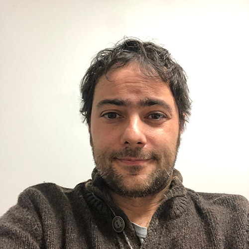
Fabrizio Guerrieri. I received my Bachelor, Master, and Ph.D. in Electronics at Politecnico di Milano in 2005, 2007 and 2010, respectively. For my doctorate research at Polimi, I designed the World’s first Single-Photon Camera. In 2009, I visited MIT for one year and used my Camera to prove a novel Quantum Imaging technique. After graduation, I joined the Functional Imaging lab at General Electric in New York, NY. There, I worked on Medical Imaging and Positron Electron Tomography (PET). In 2011 I moved to Silicon Valley to join Volterra, a startup specialized in Integrated Power Electronics and Advanced Magnetics. At Volterra, I managed a team of six Corporate Application Engineers. The Power Management circuits that my team designed are used by Lenovo Thinkpads developed from 2011 to 2013, as well as by several laptops and servers from IBM, HP, Dell, and Acer. Maxim Integrated acquired Volterra at the end of 2013. At Maxim I was a member of the Advanced R&D team, which reported directly to the CTO. My work focused on Battery Management Systems with applications in Automotive and Data Centers. HoloLens is an untethered Augmented Reality (AR) headset developed by Microsoft. I joined the then-secret team in 2016 as the Display Integration Lead. I led a cross-functional team of 10+ people from Electrical, Signal Integrity, Power, Mechanical, Display, Optics, Lasers, and Silicon engineering. HoloLens 2 shipped in 2019. The display I worked on uses RGB lasers, MEMs mirrors, and advanced waveguides to display Holograms in the user’s field of view.
In 2019 I joined Facebook as System Architect in the Oculus’ Machine Perception team. Oculus is the market and technology leader for Virtual Reality (VR) headsets. My team works on Computer Vision, 6-DoF Tracking and AI. In this highly cross-functional role, I lead a project that involves engineers from teams all over Facebook. I have fond memories of my time at Polimi. I met great people and received a World-class education that still pays dividends today. The Bachelor and Master of Electronics provided me strong and broad fundamentals that allowed me to tackle unknown disciplines and projects with ease, follow my interests, and build a fun and rewarding career.
Dennis Marco Montagna. I was born in 1969 in Pavia. I received the M.S. in Electronic Engineering in 1998 at Politecnico di Milano (POLIMI), Italy. After graduation, I joined Arca Fondi sgr as assistant for Funds Management Team with focus on quantitative analysis of portfolios and risks. From 1999 to 2002 I was Bond Fund Manager in the European Bond Team. I got also the responsibility of Corporate Bond selection for European Funds and therefore Equity Fund Manager with focus on Italian Market. In 2007 I joined the International team as portfolio manager for Nord America and International Equity Funds, developing quantitative methods and models for active fund management and options strategy. In 2014 I moved in Banca IMI asSenior Equity Portfolio Manager for Prop Desk. managing International Equities with cash & derivatives instruments applying Fundamental and Quantitative strategies. In 2016 I was in Credit Suisse Asset Management as Equities manager for Institutional Clients, in charge for global equities selection and sector allocation, with Fundamental and Quantitative strategies. In charge also for Credit Suisse Equity Italy fund (2 Lipper Fund Awards). In 2020 I’m back in Banca IMI as Capital Structure Arbitrage & Prop Desks director. Since 2012 I’m adjunct Professor for “Models and Methods for financial engineering” (former Data Processing Systems) at University of Pavia – Faculty of Economics, department of Quantitative Methods and Finance. I’m also Supervisor for several graduate Thesis in Finance, based on Alpha generation, Volatilities strategies and Portfolio selections and construction. I’m CFA Charterholder (charter awarded in June 2004) and regular member of CFA Society.
Concerning my M.S.E.E. at POLIMI, I appreciated the solid background provided by different courses. Even though tasks was demanding, I took advantage of my background in Electronics because give me flexibility and knowledge to expand my career in a different sector. First as developer of quantitative model then as analyst and portfolio manager focusing in tech sector, analysing products and industry trend.
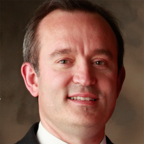
Stefano Pellerano was born in Bari, Italy, in 1977. He received the Laurea Degree (summa cum laude) and the Ph.D. degree in electronics engineering from the Politecnico di Milano, Milan, Italy, in 2000 and in 2004, respectively. During his Ph.D., his activity was focused on the design of fully integrated low-power frequency synthesizers for WLAN applications. In 2003 he has been a consultant with Agere Systems (former Bell Labs) in Allentown, PA. Since 2004 he has been with Intel Labs, in Hillsboro, OR. He is now Principal Engineer leading the Next Generation Radio Integration Lab, where he drives several research activities focused at enabling radio circuit integration in deeply-scaled CMOS technologies. His main research contributions include MIMO transceivers for WiFi, digital PLLs, high-efficient digital architectures for polar and outphasing transmitters, mm-wave radio transceiver and phased-array systems, and low-power radios. Recently, he is also exploring cryogenic CMOS integrated electronics for qubit control in fault tolerant scalable quantum computers. Stefano has authored or co-authored more than 40 IEEE conference and journal papers, one book chapter and more than 15 issued patents. He is currently serving as the Wireless Subcommittee Chair for the IEEE International Solid-State Circuit Conference (ISSCC). He served as the Technical Program Chair and General Chair for the IEEE Radio Frequency Integrated Circuit (RFIC) Symposium in 2018 and 2019 respectively and he is now part of the RFIC Executive Committee.
Rino Micheloni. I was born in 1969 in San Marino. I received the M.S. in Nuclear Engineering cum laude in 1994 at Politecnico di Milano (POLIMI), Italy. My academic CV was mainly focused on Electronics at therefore I had the opportunity to take several exams at the Department of Electronics at POLIMI.
From my graduation to 2006 I was with STMicroelectronics, working on NAND and NOR Flash memories. I joined as Junior Circuit Designer and, step by step, in 2002 I became Senior Manager for Product Development in the Joint-Venture between STMicroelectronics and Hynix in South Korea. During this time, I developed the industry’s first Multi-level NOR memory device with embedded ECC technology and the industry’s first Multi-level NAND memory with embedded BCH error correction code. After a couple of years spent in the silicon development at Infineon in Germany, in 2008 I took a step in my career and moved from a memory manufacturer to a fabless company in the US (IDT – Integrated Device Technology, Inc.) to develop microcontrollers for Solid State Drives (SSDs). At IDT I drove the architecture and design of the BCH code in the world’s first PCIe NVMe SSD controller. Over the years, SSDs have become so popular that I went through several acquisitions (IDT -> PMC-Sierra -> Microsemi -> Microchip). It is worth highlighting that from the initial value of $100M, in 2018 Microchip acquired the business for $10.4B. Today I am Vice-President and Technical Fellow at Microchip Corporation, where I run the Flash Signal Processing Labs, with special focus on NAND Flash memories, Error Correction Codes, and Machine Learning. Over my career I co-authored more than 90 publications in peer-reviewed journals and international conferences, and I hold 291 patents worldwide (including 137 US patents). I received the STMicroelectronics Exceptional Patent Award in 2003 and 2004, and the Infineon/Qimonda IP Award in 2007. In October 2019 I was nominated for the European Inventor Award 2020. Starting from 2005 I published a number of books with Springer: Inside Solid State Drives – 2nd edition (2018), Solid-State-Drives (SSDs) Modeling (2017), 3D Flash Memories (2016), Inside Solid State Drives (2013), Inside NAND Flash Memories (2010), Error Correction Codes for Non-Volatile Memories (2008), Memories in Wireless Systems (2008), and VLSI-Design of Non-Volatile Memories (2005). Concerning my M.S.E.E. at POLIMI, I appreciated the variety of teachings, the effort of all Professors in linking theory to practice, and the continuous push to look at the different topics as part of a bigger environment. Needless to say that High-Tech has changed a lot over the past 25 years but, believe it or not, I keep taking advantage of what I learnt at POLIMI. I know, studying is not easy, Professors are demanding, some subjects are boring but, if you learn with the right deepness, the toolbox that POLIMI can give you will drive you through the hurdles of your career.
Massimiliano Frulio. I was born in 1973 in Alghero (SS); I received the M.S. in Electronic Engineering in 1998 at Politecnico di Milano (POLIMI), Italy.In 1997 I joined SGS-Thomson (now STMicroelectronics) as stager for my thesis work and after my graduation I permanently joined the company; as design engineer I worked on Non-Volatile-Memories, mainly focusing on analog design. In 2001 I joined Atmel corporation; from 2001 to 2008, as flash design team leader and project leader, I worked on NVM design, developing multi-level cell NOR products and an innovative NAND flash architecture. During this time, I have authored and co-authored 21 patents. Since 2008, as design manager, I have been heading the embedded flash development for 32 bits Microcontroller products. In 2009 I have built a new design group in Shanghai, leading and mentoring the new team in Atmel-China. Since 2016, I am Senior Staff Engineer in Microchip Technology, that acquired Atmel; I am in charge of embedded flash memory design, managing a remote team in Vietnam. In my 20+ years long experience I have been working with engineers in Italy, Europe, USA, China, Vietnam and India, during all this time I appreciated the technical background I got with my M.S.E.E. at POLIMI, that gave me the ability to face new challenges and new contexts in the fast-pace changing environment of large semiconductor companies.
Maurizio Riva. I was born in 1963 Piacenza (Italy). I received the M.S. in Electronic Engineering on Oct. 29th, 1987: I remember it very well because I have been one of the 3 registered in 1982 that got it so quickly. At that time there was only one graduation lasting 5 year – 29 exams. After Graduation I started in a small IBM Personal Computer Dealer, as System Engineer installing the first Server and LAN (Local Area Networks). In 1994 I joined my first Multinational Company in LAN Software and after a couple of startups, the real jump happened in 2001 when I joined Intel Corporation, the Processors Company. I had a long career there in many roles in Italy and in EMEA (Europe Middle East and Africa), where I become EMEA Board Member and Director of Multinational Customer. I left Intel 2 years ago and I am now Vice President in charge of the EMEA Office of Quanta Cloud Technology, leader in Cloud and 5G infrastructure with Customers like Facebook and Rakuten and I relocated Düsseldorf, Germany. The M.S. in Electronic Engineer was key for my career: Planning, Organisation, Statistic and Applied Electronic to Silicon Processes gave me a real boost in helping designing Mobile Computers and Internet Infrastructure.
Francesco Magri. I was born in 1971 in Milan. After the MSc in Electronic Engineering (1996 at Politecnico di Milano), I joined the OHB Group as design engineer for onboard computer of satellites. After few years and an experience at the Group headquarter in Germany, I took an year off to study towards an MBA (2002 at INSEAD, Fontainebleau). I then started working for Dell as account manager, after a brief stint at Indesit I rejoined Dell as sales director and GM for the newly-founded Public sector. In 2012 I moved to Johnson Controls as Italy GM, the same position I took at Grundfos in 2015. At the end of 2019 I moved to USA with my family to lead a company of the Grundfos Group, Peerless Pump. We develop, manufacture and sell fire, vertical turbine and industrial process pumps globally. Electronic Engineering studies have equipped me well for the diverse challenges I have faced professionally and have allowed me to foresee and manage the spread of electronics and software to every business, including in industrial products.
Danilo Erricolo received the Laurea degree of Doctor (summa cum laude) in electronics engineering from the Politecnico di Milano, Milan, Italy, in 1993 and the Ph.D. degree in electrical engineering and computer science from the University of Illinois at Chicago (UIC), Chicago, IL, USA, in 1998. He is a Full Professor in the Department of Electrical and Computer Engineering, the Director of the Andrew Electromagnetics Laboratory, and adjunct Professor of Bioengineering at UIC. In 2017 he was nominated a University of Illinois Scholar. During the summer of 2009, he was an Air Force Faculty Fellow at the Air Force Research Laboratory, Wright-Patterson Air Force Base in Dayton, OH, USA. He has authored or coauthored more than 275 publications in refereed journals and international conferences. His research interests are primarily in the areas of antenna design, electromagnetic propagation and scattering, high-frequency techniques, wireless communications, electromagnetic compatibility, the computation of special functions, and magnetic resonance imaging. In 2016 he was elevated to Fellow of IEEE for “contributions to electromagnetic scattering associated computational algorithms.”
Dr. Erricolo was elected Full Member of Commissions B, C and E of the U.S. National Committee (USNC) of the International Union of Radio Science (URSI), a committee of the US National Academies. He served as Chair (2009-2011), Vice Chair (2006-2008) and Secretary (2004-2005) of the USNC-URSI Commission E on Electromagnetic Environment and Interference. He was Chair of the USNC-URSI Ernest K. Smith Student Paper Competition (2009-2014); Vice-Chair of the Local Organizing Committee of the XXIX URSI General Assembly, held in Chicago, IL, USA in August 2008; and Member at Large of USNC-URSI (2012-2017). He was the General Chairman of the 2012 IEEE International Symposium on Antennas and Propagation and USNC-URSI National Radio Science Meeting, held in Chicago, IL, USA in July 2012. He was an Elected Member of the IEEE AP-S Administrative Committee (2012-2014); Chair of the IEEE AP-S Distinguished Lecturer Program (2015-2016); and Chair of the Chicago Joint Chapter of the IEEE AP-S and Microwave Theory and Techniques Society (2011-2016). He has served on more than 40 conference technical program committees, chaired over 60 conference sessions and organized more than 20 special sessions at international scientific conferences. He has been the Editor-in-Chief of the IEEE TRANSACTIONS ON ANTENNAS AND PROPAGATION since August 2016.
Tommaso Frizzi was born in 1978 and received the M.S. in Telecommunication Engineering in 2003 and the Ph.D. degree in “ICT” in 2007, both at Politecnico di Milano, Italy.
After graduation I joined the laboratories of the Department of Electronics and Information of the Politecnico di Milano, group of Prof. A. Longoni. I had been dealing with the design of the front-end electronics for X-ray detectors as part of an international experiment of hadronic physics. Later I won a fellowship grant related to the control electronics of MEMS accelerometers, still at POLIMI.
Basing on my knowledge in the radiation detection and the MEMS fields, I started-up two companies, XGLab SRL (2009) and ITmems SRL (2013), both as spin-off of Polimi. I am currently Vice President of “X and Gamma Components” business unit at Bruker Nano Analytics (bruker.com) and Managing Director at XGLab (xglab.it). During my experience as a student at Polimi I have met many valuable people, many of those still cooperating with me in my new business adventure.